
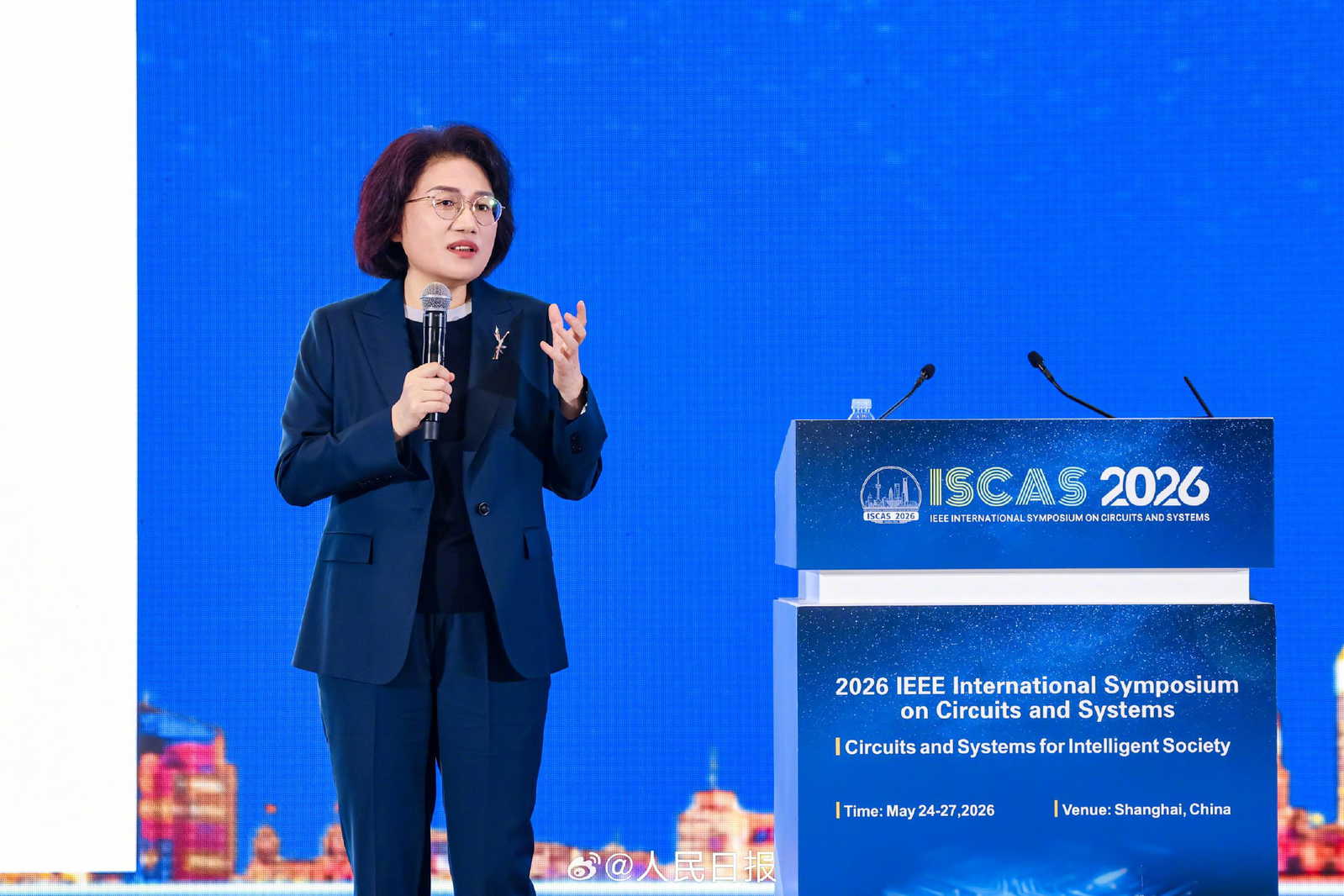
Huawei Technologies said on Monday in Shanghai that it will pursue a new chip-design strategy it believes can deliver industry-leading semiconductors within five years, even as US sanctions restrict China’s access to advanced chipmaking tools.
The company said its high-end chips should reach transistor density equivalent to 1.4-nanometre processes by 2031, but it did not present independent performance data.
Also Read | Tesla plans expansion in Hyderabad with new sales, service hub
HUAWEI has presented the Tau (τ) Scaling Law, a new principle for guiding the future development of the semiconductor industry. By 2031, HUAWEI's high-end chips based on this law are expected to feature a transistor density that is equivalent to 14 (1.4 nm) processes.
— Huawei (@Huawei) May 25, 2026
The race grows frightfully tight
The target matters because China’s most advanced proven chipmaking capability is widely seen at about 7 nanometres, while 1.4 nanometres is expected to sit near the global frontier by the end of the decade.
Taiwan Semiconductor Manufacturing Co (TSMC), the world’s largest advanced-chip producer, is currently using 2-nanometre technology and plans to begin mass production of 1.4-nanometre chips in 2028.
He Hui, director of semiconductor research at Omdia, said, “What Huawei is proposing is a shift from traditional node-driven scaling to system-level efficiency scaling.”
Huawei claims its new LogicFolding approach can help narrow the gap with $TSM by improving chip density, latency & power efficiency without relying only on smaller transistors.
— Shay Boloor (@StockSavvyShay) May 25, 2026
TSMC already attacks this problem through CoWoS-L & SoIC packaging with $NVDA, $AMD, $AVGO, $QCOM &… pic.twitter.com/N3OwxFaqGM
Now comes the clever machinery
Huawei’s new principle, called the Tau Scaling Law, is aimed at reducing the time it takes signals and data to move through chips and computing systems.
The company said its Kirin smartphone chips due later this year will be the first to use a related architecture called LogicFolding, which it said will shorten wiring inside chips and improve performance.
Huawei added that LogicFolding will also be applied to Ascend chips by 2030 and to large AI clusters used in data centres.
Huawei's latest announcement carries real significance, because China has, in effect, shown the direction in which advanced technology needs to move. And it has done so in cutting-edge semiconductors, no less.
— Jukan (@jukan05) May 25, 2026
China has long been a follower. In semiconductors, Western technology… pic.twitter.com/tmleGrFDOi
Sanctions, setbacks and a stubborn revival
The company said its chip division has designed and mass-produced 381 chips over the past six years based on the Tau Scaling Law for use in smartphones and AI computing.
Huawei’s Ascend chip line is central to powering Chinese AI models, while demand for those chips has risen in China as firms look for alternatives to Nvidia’s restricted products.
Analysts cited by Reuters said the approach could narrow the gap with global leaders, but significant hurdles remain, including overheating, cost and system integration.
Huawei was placed on a U.S. trade blacklist in 2019, and the company staged a comeback in 2023 with its Mate 60 series smartphones powered by a 7-nanometre chip made by SMIC; SMIC shares rose 7.6% after Huawei’s announcement.